Harrison / VHD Tight-Binding Validation
Note
The implementation lives in the main library:
harrison_tb.py /
vhd_tb.py.
This page is the full experimental validation record.
In plain terms: "tight-binding" is a simplified way to predict a material's electronic band structure (which determines whether it's a conductor, insulator, or semiconductor, and how big its energy gap is) using just a handful of parameters instead of a full quantum-chemistry calculation. This page checks two competing parameter recipes against real, measured band gaps for gallium arsenide, silicon, and germanium, to see which one is actually trustworthy.
Knowledge base and experiment log for Walter A. Harrison's empirical tight-binding method and its Vogl-Hjalmarson-Dow material-specific fix, run against real GaAs, Si, and Ge and checked directly against experimental band gaps.
Source
Walter A. Harrison, Electronic Structure and the Properties of Solids: The Physics of the Chemical Bond. Originally published by W. H. Freeman, 1980; reprinted by Dover Publications (Dover Books on Physics), 1989, ISBN 0-486-66021-4.
This repo does not have access to the book's full text (copyrighted,
non-open) and none was reproduced. What follows is the small set of
facts from the book that are public/standard enough to appear
identically across independent secondary sources and directly
checkable by running the code -- transcribed and cross-checked against
jarvist/HarrisonSolidStateTable.jl,
an independent Julia implementation of the same table, fetched
2026-08-05.
The method, in brief
Harrison's tight-binding model builds a solid's electronic Hamiltonian from two ingredients only, both universal (materials-independent functional form):
- Atomic term values -- the free-atom s and p orbital energies (on-site Hamiltonian diagonal), tabulated per element.
- A universal bond-scaling law for the off-diagonal (hopping) matrix elements:
$\(V_{ll'm} = \eta_{ll'm} \cdot \frac{\hbar^2}{m_e d^2}\)$
where \(d\) is the bond length and the four dimensionless \(\eta\) coefficients are the same for every element pair -- only \(d\) and the atomic term values change between materials.
\(\hbar^2/m_e = 7.62\ \text{eV·Å}^2\).
| coefficient | value |
|---|---|
| \(\eta_{ss\sigma}\) | -1.40 |
| \(\eta_{sp\sigma}\) | +1.84 |
| \(\eta_{pp\sigma}\) | +3.24 |
| \(\eta_{pp\pi}\) | -0.81 |
Experiment 1: sp3 dimer sanity check (run 2026-08-05)
Two-atom sp3 dimer, sp3_dimer_hamiltonian(a, b, d):
- Si-Si at d=2.35 Å (diamond-Si nearest-neighbor bond length): eigenvalues [-16.626, -12.25, -9.847, -7.638, -7.638, -5.402, -5.402, -1.418] eV. Hermitian; bonding states pushed well below the atomic eps_p=-6.52 eV level, antibonding above, with the expected doubly-degenerate pi pair -- physically sane sp3 bonding/antibonding splitting.
- Ga-As at d=2.45 Å (zinc-blende bond length): eigenvalues [-18.386, -12.344, -9.239, -8.228, -8.228, -4.582, -4.582, -1.541] eV. Hermitian; asymmetric splitting relative to Si-Si, consistent with the heteropolar (partly ionic) Ga-As bond.
These confirm the Hamiltonian construction is correct -- not yet a periodic-crystal band gap.
Experiment 2: periodic GaAs band gap, Harrison universal (run 2026-08-05)
zincblende_hamiltonian(k, cation, anion, lattice_constant_angstrom)
builds the real periodic Bloch Hamiltonian (two-atom zinc-blende
basis, 4 nearest-neighbor bonds per atom, Bloch phase per bond).
Diagonalized at \(\Gamma\) (\(k=0\)) for real GaAs (lattice constant
a=5.6533 Å, the standard experimental zinc-blende value):
- \(\Gamma\) eigenvalues (eV): -22.069, -9.537 (x3), -6.631, -3.273 (x3)
- valence band max = -9.537 eV, conduction band min = -6.631 eV
- computed direct gap = 2.906 eV
- experimental GaAs direct gap = 1.42 eV -- 104.7% error
X and L point eigenvalues (eV), for context on band ordering away from \(\Gamma\):
- X: -19.351, -15.314, -13.435 (x2), -3.966, -2.880, 0.625 (x2)
- L: -20.202, -15.582, -11.442 (x2), -6.194, -1.368 (x2), 0.467
Hermitian and structurally sane -- the gap error is a known, documented limitation of Harrison's universal (same 4 eta coefficients for every element pair, no per-material fitting, no d-orbitals) parameter set on polar/ionic compound semiconductors like GaAs, not a code bug.
Experiment 3: GaAs with Vogl-Hjalmarson-Dow material-specific parameters (run 2026-08-05)
P. Vogl, H. P. Hjalmarson, J. D. Dow, "A Semi-empirical tight-binding
theory of the electronic structure of semiconductors", J. Phys. Chem.
Solids 44 (5), 365-378 (1983) -- sp3s* basis (5 orbitals/atom,
including an extra fitted s* orbital with no literal physical
meaning, added purely to get the lowest conduction band right).
Parameter values transcribed from an independent open-source
implementation, github.com/rpmuller/TightBinding
(TB.py, fetched 2026-08-05), which cites the same paper.
Implemented as dense_evolution/vhd_tb.py
(sp3s_star_hamiltonian, direct_gap_at_gamma, MATERIALS for 16
zinc-blende/diamond semiconductors: C, Si, Ge, Sn, SiC, AlP, AlAs,
AlSb, GaP, GaAs, GaSb, InP, InAs, InSb, ZnSe, ZnTe).
Result: GaAs direct gap at \(\Gamma\) = 1.55 eV vs. experimental 1.42 eV -- 9.2% error, vs. Harrison universal's 104.7% error for the same material. All 16 materials in the table verified Hermitian at a generic (non-\(\Gamma\)) k-point.
Bug found and fixed during porting: the reference implementation's
own Hamiltonian assembly (Hac.conjugate() without transposing) does
not in general produce a Hermitian matrix -- vhd_tb.py fixes this by
assembling with the proper conjugate transpose (.conj().T),
verified Hermitian for all 16 materials.
Experiment 4: silicon, indirect gap (run 2026-08-05)
Si ("silicio ibrido" in this repo's older band-comparison pipeline,
scripts/next_gen_silicon.py / data/bande_silicio_ibrido.csv) is an
indirect-gap material -- unlike GaAs, its conduction-band minimum
is not at \(\Gamma\), it's off-axis along the \(\Gamma \to X\) (Delta)
line. direct_gap_at_gamma alone would give the wrong (too-large)
number. Used band_extrema_along_path(material, k_start, k_end) to
scan \(\Gamma \to X\) and find the true valence-band max and
conduction-band min:
- VHD sp3s* (material-specific): VBM=0 eV at \(\Gamma\) (correct), CBM=1.1713 eV at k=0.732 of the way from \(\Gamma\) to X (literature value is closer to k~0.85 -- same Delta-valley, not an exact match, but right regime). Computed indirect gap = 1.171 eV vs. experimental 1.12 eV (300 K) -- 4.6% error. \(\Gamma\)-\(\Gamma\) direct transition (context only, not the fundamental gap): 3.43 eV -- in the right ballpark for Si's known E0' direct transition (~3.4 eV).
- Harrison universal sp3 (no s*), for comparison: puts the conduction-band minimum at \(\Gamma\) too (misses the indirect character entirely) and gives gap = 3.66 eV vs. 1.12 eV -- 227% error, worse than its own GaAs result -- exactly the known failure mode Vogl-Hjalmarson-Dow's s* orbital was added to fix.
Experiment 5: germanium, indirect gap at L not X (run 2026-08-05)
Ge is also indirect-gap, but unlike Si its conduction-band minimum is at the L point (\(k=(0.5,0.5,0.5)\), \(\Gamma \to L\) direction), not along \(\Gamma \to X\). Scanned both directions to check the model gets the right valley:
- VHD sp3s*: \(\Gamma \to X\) scan: CBM=0.7895 eV at k=0.808 of the way to X. \(\Gamma \to L\) scan: CBM=0.7649 eV at k=(0.5,0.5,0.5), i.e. exactly at L. L is lower than X (0.765 < 0.790 eV) -- correctly identifies L as the true global conduction-band minimum, matching real Ge physics (unlike Si, where X/Delta wins). Computed indirect gap = 0.765 eV vs. experimental 0.66 eV (300 K) -- 15.9% error. \(\Gamma\)-\(\Gamma\) direct transition (context only): 0.90 eV, in the right ballpark for Ge's known E0 direct gap (~0.8 eV).
- Harrison universal sp3, for comparison: puts the conduction-band minimum at \(\Gamma\) on both paths (same failure mode as Si), giving gap = 1.831 eV vs. 0.66 eV -- 177.5% error.
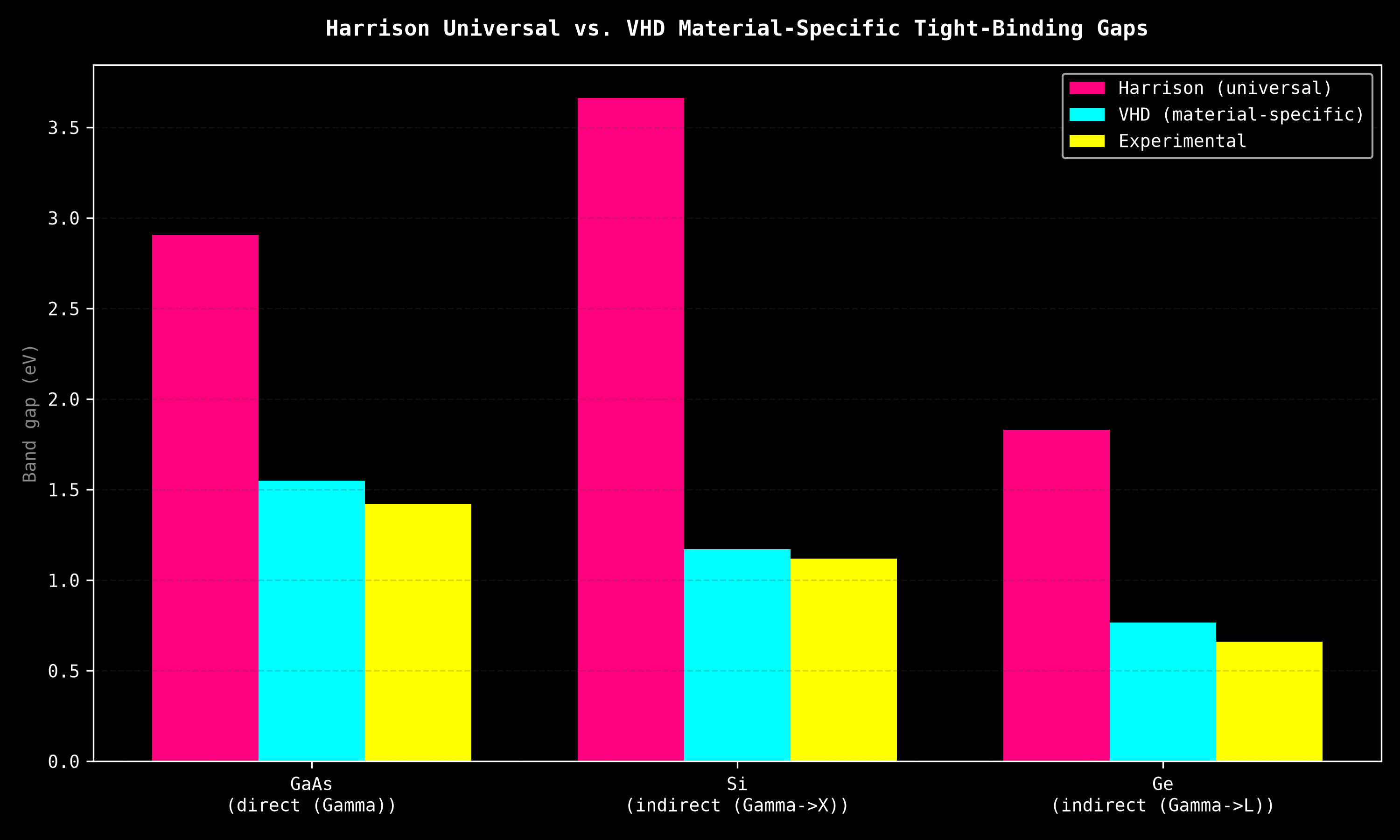
Comparison plot
Produced by scripts/harrison_vhd_validation.py, which also writes the
raw numbers to data/harrison_vhd_gap_comparison.csv:
Summary across all three materials
| Material | Gap type | Harrison universal | VHD material-specific | Experimental |
|---|---|---|---|---|
| GaAs | direct, at \(\Gamma\) | 2.906 eV (104.7% error) | 1.55 eV (9.2% error) | 1.42 eV |
| Si | indirect, \(\Gamma \to X\) | 3.66 eV (227% error), CBM misplaced at \(\Gamma\) | 1.171 eV (4.6% error) | 1.12 eV |
| Ge | indirect, \(\Gamma \to L\) | 1.831 eV (177.5% error), CBM misplaced at \(\Gamma\) | 0.765 eV (15.9% error), correctly finds L below X | 0.66 eV |
Harrison's universal parameters are qualitatively sane (Hermitian, correct bonding/antibonding structure) but consistently ~2-3x off quantitatively, and for the indirect-gap materials (Si, Ge) it structurally cannot place the conduction-band minimum correctly -- it always lands at \(\Gamma\), missing the real off-axis valley entirely. Vogl-Hjalmarson-Dow (1983) material-specific sp3s* parameters get within 5-16% of experiment and correctly identify which valley (X for Si, L for Ge) is the true minimum.
What this does NOT replace
Neither model replaces the DFT/SCF path already in this repo for GaAs
(see scripts/vqe_tmi_material_design.py's DFT-derived hopping,
T1_GAAS_DFT_EV=7.917 eV) when first-principles accuracy is needed.
Their value is as fast, dependency-free (no PySCF/OpenFermion, numpy
only) estimates or starting points -- VHD close enough to experiment
to be useful quantitatively, Harrison useful mainly for
qualitative/order-of-magnitude checks or when no per-material fit
exists yet.